Table of Contents
Introduction
A static protective relay refers to a relay in which the measurement or comparison of electrical quantities is done in a static network which is designed to give an output signal in the tripping direction when a threshold condition is passed. The output signal operates a tripping device which may be electronic, semiconductor, or electromagnetic.
Basis for Static Relay Development
As a result of the great expansion of electrical transmission and distribution systems during the last thirty years and with the advent of much larger power stations and more highly interconnected systems, the duty imposed upon protective gear has become more and more severe. Since relays now have to perform much more complicated functions many types tend to become very complex mechanically and hence costly and difficult to test and maintain.
The basis of the so-called static relaying is the use of circuits and components to achieve a variety of functions and operating characteristics which for protection purposes have traditionally been obtained using electromechanical devices. Reliability, always important has been emphasized as snort-circuit levels, circuit ratings and complexity of interconnection have increased. Shorter operating times have become more essential to preserve dynamic stability as the character and loading of systems approach design limits. The satisfaction of these requirements has left little potential for further improvements in conventional electromechanical relays Until fifteen years ago, relay design was dominated by the use of electromechanical elements. Such an element of whatever basic characteristics, e.g., square law induction element has a dynamic behavior special to that element and design freedom is consequently restricted by factors such as the conflicting requirements of sensitivity and mechanical robustness. Experience shows that these more exacting requirements can readily be met using new static relays.
Classification of Static Relays
Static relays are classified according to the type of measuring unit or the comparator as follows:
(1) Electronic relays
(ii) Transductor (magnetic amplifier) relays
(iii) Rectifier bridge relays
(iv) Transistor relays
(v) Hall effect relays
(vi) Gauss effect relays.
1. Electronic Relays
These were the first to be developed in the series of static relays. They date back to early 1928 when Fitzgerald presented a carrier current pilot relaying which constituted unit protection of the transmission line. Subsequently, a series of electronic circuits for most of the common types of protective gear relays were developed. The components used were electronic valves for measuring units.
The two basic arrangements are one as an amplitude comparator and another as a phase comparator. In the former case two a.c. quantities to be compared are rectified and applied in opposition in the control grid circuit of an electronic tube so that operation occurs when one quantity exceeds the other by an amount depending on the bias. In the latter case one a.c. quantity can be connected to the control grid of an electronic tube and the other a.c. quantity to the screen grid of the tube, the operation occurs when the two quantities are in phase. Electronic relays offer the following advantages:
(a) Low burden on CTs and PTs, since the operating power is from an auxiliary d.c. supply.
(b) Absence of mechanical inertia and bouncing contacts.
(c) Fast operation.
(d) Low maintenance, owing to the absence of moving parts.
Despite all these however electronic relays have not met with general success except for carrier current relaying which has attained widespread use. The major reason is that carrier relaying has accomplished a highly desirable result not economically feasible by any other method. This popularity is despite the following limitations of the electronic circuits.
(a) Presence of incandescent filament and the necessary low-voltage power supply to heat them.
(b) Short life of the electronic valves.
(c) High power consumption.
(d) Requirement of high-tension supply.
(e) High cost for simple relays such as overcurrent relays.
2. Transductor (Magnetic Amplifier) Relays
Since relays now have to perform much more complicated functions, many types tend to become very complex mechanically, and hence costly to make and difficult to test and maintain. The transductor controlling a simple slave relay makes it possible to reduce a complex electromechanical device that operates by the interaction of fluxes and currents in a fully predictable way.
A transductor comprises essentially a magnetic core on which there are two groups of windings, usually known respectively as the operating windings and control windings. Each group may comprise only one winding but if there is more than one winding in a group all those windings are magnetically linked. On the other hand, the windings of the different groups are not magnetically linked. The operating windings are energized with a.c. and control windings are energized with d.c. A transductor operates to present a variable impedance to currents flowing in the operating windings the magnitude of this impedance being varied by the current in the control winding.
If used as an amplitude comparator it is limited in its sensitivity by the sensitivity of the slave relay in its output circuit; if used as a phase comparator to obtain greater sensitivity it is dependent upon an external a.c. supply which is sometimes difficult to arrange.
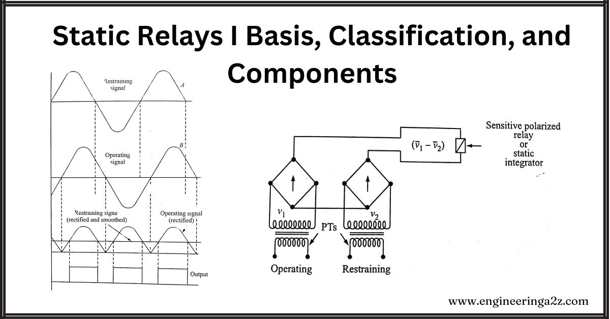
A transductor relay where the restraining voltage is applied to the control winding through an impedance Z and a rectifier. The restraining current thus obtained is rectified and partially smoothed by the short-circuit effect of the rectifier on the control winding and also due to the short-circuited coupling winding. The effect of this is to drive both the limbs on which the operating winding is wound into saturation.
Now the operating winding is wound in such a way that the operating ampere-turns oppose the restraining ampere-turns in one limb and reinforce them in the other. Neglecting the finiteness of permeability and assuming equality of restraining and operating turns, the operating current would drive out of saturation, the limb in which the operating current is against the restraining ampere-turns when the peak value of the operating current exceeds the magnitude of the restraining current. When this happens a voltage is induced in the output winding and the relay is energized. The same operation is repeated on the other limb during the next half cycle.
The slave relay current is very low until the above-mentioned condition exists. Then it suddenly increases and becomes very large for a small value of operating current. For this reason, a heavy-duty telephone type of relay is used with large settings. Due to smoothing and rectifying a signal, a delay is introduced because of the time constant of the smoothing circuit and hence the operating speed is slow. Transductor relays are mechanically very simple and although some of them may appear to be a little complicated electrically, this does not affect their reliability adversely, since their operation is mainly dependent on static components whose characteristics are easily predetermined and checked. As a result, they are easier to construct and test than electromechanical relays and their maintenance is practically negligible.
3. Rectifier Bridge Relays
With the development of semiconductor diodes, this type has gained popularity and consists of two rectifier bridges and a moving coil or polarized moving iron relay. The most common are relay comparators based on rectifier bridges, which can be arranged as either phase or amplitude comparators.
4. Transistor Relays
These are the most widely accepted types of static relays, so much so that when we say static relays, we can safely infer transistor relays only. The transistor which acts like an electronic valve can overcome most of the limitations posed by electronic valves and thus has made it possible to develop electronic relays more commonly known as static relays.
The characteristics of modern transistors are such that they can replace the functional elements that are used in electromechanical relays to give necessary characteristics. The technical features particularly suited to the design of functional units include amplifying and switching characteristics, sensitivity and high speed Experience has shown that transistor circuits cannot only perform the essential functions of a relay such as summation, comparison of inputs, and integrating them, but they also provide the necessary flexibility to suit the various relay requirements.
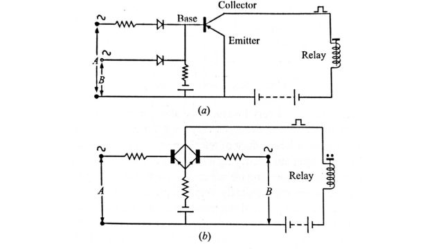
Two basic arrangements of relays based on transistor comparators are shown in Fig. In either of these circuits, current of constant magnitude flows in the collector circuit only when the input a.c. quantities are simultaneously negative; a relay in the collector circuit will pick up when the overlap angle exceeds a certain value, ie., when the mean d.c. level in the collector circuit exceeds the relay pickup as a result of phase coincidence.
The advantages of transistorized relays may be enumerated as follows:
(a) Quick response, long life, high resistance to shock and vibration.
(b) Quick reset action a high reset value and absence of overshoot is easily achieved because of the absence of mechanical inertia and thermal storage.
(c) No bearing friction or contact troubles (no corrosion, bouncing, or wear), so minimum maintenance is required.
(d) The ease of providing amplification enables greater sensitivity to be obtained.
(e) The basic building blocks of semiconductor circuitry permit a greater degree of sophistication in the shaping of operating characteristics, enabling the practical realization of relays with threshold characteristics more closely approaching the ideal requirements.
(f) The low energy levels required in the measuring circuits permit miniaturization and minimize current transformer inaccuracies.
(g) Use of printed (or integrated circuits) to avoid wiring errors and to facilitate rationalization of batch production.
Static relays employing transistors have their limitations which are:
(a) Variation of characteristics with temperature and age.
(b) Dependence of reliability on a large number of small components and their electrical connections.
(c) Low short-time overload capacity compared with electromagnetic relays.
It has now become possible to compensate for all these factors. For example, the use of thermistors eliminates temperature error, whilst aging may be minimized by presoaking for several hours at a relatively high temperature. Factors (b) and (c) above are the design features of the circuit and careful design can compensate for these limitations.
5. Hall Effect Relays
Hall effect is utilized to give a phase comparator. The effect is very predominant in certain semiconductors such as indium arsenide, indium antimonide, indium phosphate, etc. The basic Hall generator where the Hall crystal in the form of a slab carries current in the X-direction and is placed in a magnetic field in the Y-direction, a voltage known as Hall voltage is induced in the Z-direction across the edges of the crystal.
6. Gauss Effect Relays
Some semiconductors have the property where the resistance varies when the magnetic field is applied. This effect is known as magneto resistivity or Gauss effect. If one a.c. voltage V₁ produces the magnetic field through the crystal, which for the best results should be in the form of a disc having a large diameter and another voltage V₂ sends a current radially through the disc, then the current will be proportional to V₁₂ cos 0, where 9 is the angle between the two voltages. This can thus act as a phase comparator and be used as a static relay. This is however better than Hall effect devices because polarizing current is not required, the crystal is simpler and the output is higher. The cost of the crystal has limited its use in static relays.
Basic Components of Static Relays
Some of the commonly used components in static relays are discussed below.
- Semiconductor Diodes
- Transistors
- The Field – Effect Transistor (FET)
- Unijunction Transistor ( UJT)
- Thyristor
- Logic Circuits
- Smoothing Circuits
- Voltage Regulators
- Square – Wave Generators
- Time Delay Circuits
- Level Detectors
- Summation Devices
- Sampling Circuits
- Zero Crossing Detector
- Output Devices
1. Semiconductor Diodes
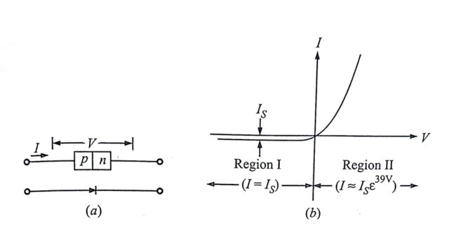
The pn junction has rectifying characteristics as shown in Fig. If a source of emf is connected to the pn junction in the polarity shown in Fig, then the spare holes in the p-type region are drawn easily to the negative pole, and the electrons are drawn from the n-type to the source positive. If the source potential is reversed then the holes are repelled from the positive pole and likewise the electrons from the negative pole. Consequently, little current flows until the electric stress is so high that a process similar to an electric discharge occurs.
The approximate static behavior of either the silicon or germanium pn junction diode is given by:
I = IS (εVq/KT – 1)
where
- IS = reverse saturation current, amperes
- V = applied voltage in volts
- q = charge on electron (1.59 × 10⁻¹⁹ C)
- K = Boltzmann’s constant (1.37 × 10⁻²³ W-S/°K)
- T = Absolute temperature, degrees Kelvin
At the normal room temperature of about 300°K
I = IS (ε39V – 1)
In the forward direction, when I become larger than a few tenths of a volt, the forward current becomes
I ≅ IS ε39V
Correspondingly, in the reverse direction, the current expression becomes
I ≅ -IS
In the reverse direction, the silicon diode has a very small reverse current which increases slowly as V is made more negative until a critical or breakdown voltage is reached. The voltage at which this breakdown occurs is controllable in the manufacture of diodes, and a variety of diodes are commercially available with breakdown voltages from about 2 V to 2,000 V. In a rectifier circuit, the reverse breakdown is undesirable, and the diode is chosen to have a higher breakdown voltage than any voltage likely to appear across it. In other applications, the breakdown is used, and the diode is chosen for a specific voltage. Diodes so used are variously called zener, avalanche, regulator, reference, or just breakdown diodes.
The practical semiconductor diodes fall short of the ideal in three respects.
(a) They do not provide a perfect short circuit in the forward (Region II) direction.
(b) They do not provide a perfect open circuit in the reverse (Region 1) direction.
(c) They possess inertial effects, i.e., the voltage or current cannot change instantaneously from one value to another, for instance, certain of the semiconductor devices are relatively slow to switch from on to off (Region II to Region I)
2. Transistors
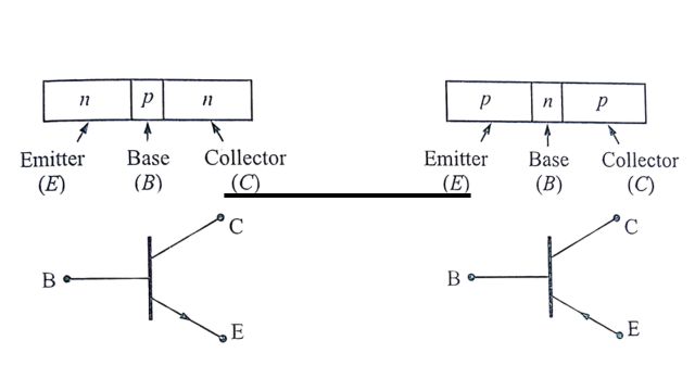
In its simplest form, it consists of two pn junction diodes coupled together by a very thin common base, either of p-type or n-type semiconductor material. It is possible to separate input and output circuits, which may be controlling circuits and controlled circuits respectively. It has many advantages like small size, ruggedness, absence of filament heating power, etc., as compared to vacuum tubes.
Another main advantage of transistors is that it can be made in two types; pnp transistors in which a region of n-type is sandwiched between two regions of p-type and vice versa in npn-type. The symbolic representation and the nomenclature used are shown in Fig.
(a) Transistor as a Switch
The switching capabilities of a transistor stem from the capability of the device to rapidly change the d.c. resistance between its output terminals, the collector and emitter, from a very high to a very low value, in response to a small current injected into the control (base) terminal.
A schematic of a basic transistor switching circuit is shown in Fig. A voltage pulse (Vi) applied to the input terminal causes a current flow (iB) through the base resistance (RK) which in turn reduces the collector-emitter resistance to a very low value and permits a large current flow (ic) from the battery through the load. The transistor gets saturated and operates in Region III. If the input voltage is removed, the reverse bias voltage (VOB) causes the collector-emitter resistance to increase greatly, and significantly the load current. Transistors, though they fall short of perfection represent the best available components for switching applications, especially in high-speed equipment. Factors that prevent a transistor from duplicating an ideal switch are:
(a) A residual leakage current when the transistor is off.
(b) A residual collector-emitter saturation voltage when the transistor is on.
(c) Time delays involved in the response of collector current to changes in the input signal
(b) Transistor Amplifiers
There are three basic methods of connection of a transistor in an amplifier circuit. Figure shows these connections for both pnp and npn transistors. The emitter-base junction is always forward-biased and the collector-base junction is always reverse-biased. By sending a current through the emitter-base junction at a low voltage, almost the same amount of current is made to flow in the comparatively high-voltage collector circuit. This accounts for the power amplification achieved. Because of its high gain, the common emitter circuit is most commonly used.
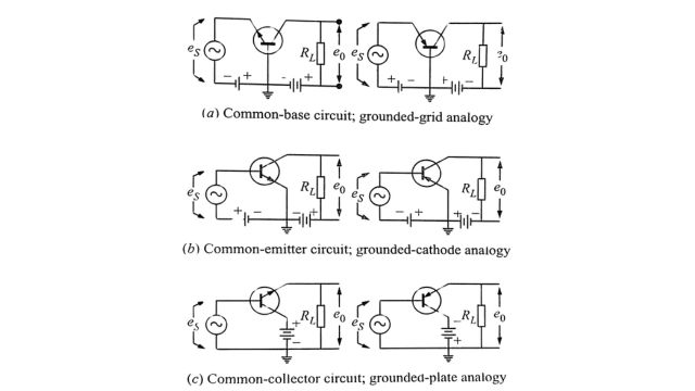
The fact that current amplification is linear, whereas the voltage amplification depends upon the load impedance, means that transistor amplifiers are linear only as current amplifiers, ie., the input must be a current source or the source impedance must be high compared with the transistor input impedance if a voltage source is used.
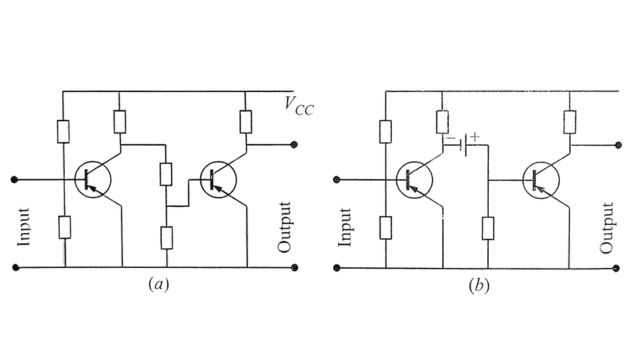
(c) D.C. Amplifiers
These are amplifiers that have zero frequency as the lower band limit to retain the initial displacements, d.c. components and low-frequency transient offsets that may accompany the a.c. and time-varying signals. It is not possible to use reactive coupling elements to separate signals and bias quantities. Any drift in the quiescent operating values cannot be distinguished from signals that are to be amplified. Direct-coupled amplifiers, therefore, have special problems in long-term stability.
The main reasons for the drift are:
(i) variation of emitter-to-base voltage,
(ii) variation in the gain of the transistor and
(iii) variation in the power supply voltage.
Temperature variation is one of the main causes of these variations. Numerous compensation techniques and circuits have been developed and are in use. Two principal schemes of direct-coupled amplifiers are shown in Fig. The only difference between the two schemes is that the resistance potential divider of Fig. is replaced by a battery in series with a resistance in Fig.
An alternative method is to use a chopper which converts a slowly varying direct current to an alternating form, which is amplified by an a.c. amplifier and its output is either used in a.c. form or rectified back to direct current again.
Typical transistor chopper circuits are shown in Fig. The circuit shown in Fig is suited for general use. When the base is driven positive by the square-wave output of the driving transformer, the transistor closes the circuit and the d.c. input voltage appears across R2. When the base is driven negative, the transistor is switched open and the voltage across R2 is zero. The circuit uses two transistors, and it is useful with -resistance sources since it has an on-off switch in series and an off-on switch in shunt with the source. When TA is on, the collector-to-base junction of TB is reverse-biased, and for source. When half cycle of switching frequency, when TB is on, the junction of TA is reverse-biased.
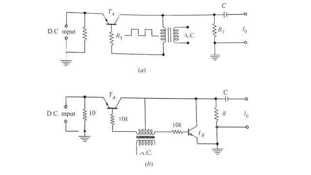
The leakage current of TA is shorted out of the load by TB during the half cycle in which TA, is open, and the leakage current of TB passes largely through TA on the reverse half cycle, if R is large. The offset or threshold voltages of both transistors are identically applied across R on successive half cycles, but this voltage does not reverse and thus acts as a d.c. component which is removed by C.
3. The Field – Effect Transistor (FET)
The field-effect transistor (FET) is a unipolar device as compared to the bipolar transistor already discussed. It consists of a bar of semiconductor material whose resistance is modulated by varying either the cross-sectional area of the bar or the density of current carriers in it, or both, by some electrical means. Two structures are used. One is an all-junction device in which the controlled modulation involves only the cross-section of the conducting channel. This is usually called junction FET. The other structure, called an insulated-gate FET (IGFET) or metal-oxide silicon FET (MOSFET) involves modulation of both the channel cross-section and the density of current carriers in it.
Junction FET is illustrated in cross-section in Fig. An n-type bar of germanium is flanked by two regions of p-type germanium. The conduction current to be modulated is carried between the ends of the n-type bar. The cross-sectional area available for conduction between the two p-type regions is a function of the magnitude of the reverse bias between the two p-type regions and the n-type bar, The input impedance of this device is quite high, and the output impedance in moderately high.
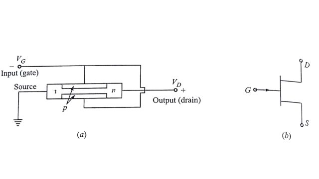
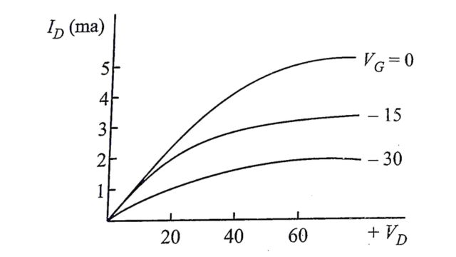
This type of device shows less internal feedback between the input and output than the conventional transistor. Typical characteristic curves of junction FET are shown in Fig. (10.12). It has characteristics similar to a pentode tube. A few volts of negative bias on the gate blocks the current between the drain and source by the field effect.
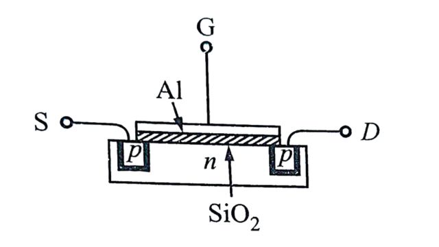
The MOSFET structure is shown in Fig. Here it can be seen that two diffused p-regions, the source and drain are separated by the n-type material of the starting crystal. On top of this insulating oxide between the source and drain regions, a metal gate electrode of aluminum is deposited. Aluminum contacts are also made to the source and drain regions. If a negative charge of several volts is placed upon the gate electrode, an equal positive charge will gather on the surface of the semiconductor crystal just beneath the oxide. This positive charge now connects the p-type source and drain regions, and since it is mobile it forms a thin conducting channel between them. It has a very high input impedance. The major advantage of the device is that the high input impedance is retained for either a positive or negative input voltage since the gate is insulated from the rest of the structure by the SiO₂ layer. This behavior contrasts with the junction FET where the gate is a reverse-biased junction for one input polarity but a forward-biased junction for the other input polarity.
(a) The FET as a Switch
At low frequencies, the FET has no offset voltage. There is no threshold required for the signal to be switched. In an ordinary bipolar transistor, the signal being switched must exceed the voltage of the knee in the forward diode characteristic of the collector before there is an appreciable signal through the switch in the on state. Here the channel, when opened by the gate, is a linear resistance requiring no such threshold. At a high frequency of switching, there is a current due to the rapid charging and discharging of the gate capacitance through the channel, creating an IR drop in the channel which acts like an offset voltage.
4. Unijunction Transistor ( UJT)
It is a three-terminal device with only one pn junction. It is made up of an n-type silicon wafer having two base controls and a p-type alloy junction which acts as an emitter electrode. In normal operation, the lower ohmic contact (base B1) is grounded. If the emitter junction is left open circuit, the voltage between B1 and B2 sets up a current proportional to the conductance of the wafer. The base B2 is made positive concerning B1, by voltage VBB and a fraction η of this voltage appears between the emitter E and B1. Under the conditions of no current in the emitter, the UJT between B1 and B2 has the characteristics of an ordinary resistance called the interbase resistance RBB. At 25°C this resistance lies between 4 and 10 KΩ and increases linearly with temperature up to about 140°C. The normal biasing conditions for the UJT and its symbol are indicated in Fig. If VE applied is less than η VBB, the emitter will be reverse biased, and only leakage current will flow. If VE is greater than η VBB the junction becomes forward-biased and a large emitter current flows with a low forward voltage drop between the emitter and B₁.
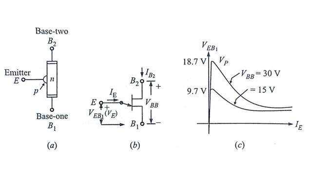
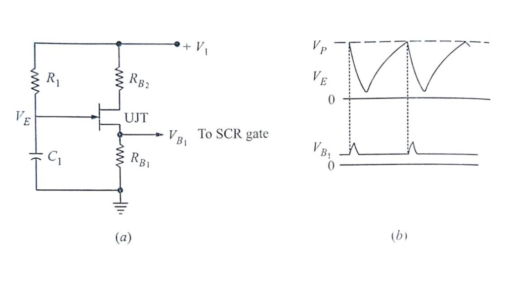
The characteristics show that there is a large negative resistance region for fast-switching action. The use of UJT is in generating trigger input to SCRs. For such an application, the basic circuit of Fig is used. The capacitor C1 charges through R1 until VE reaches the peak-point voltage VP when the UJT triggers and discharges C1 through RB1. When VE reaches a low value, perhaps 2 V, the capacitor can no longer supply the necessary emitter-base current, and UJT turns off. Base resistor RB provides an output-voltage pulse during the very short high-current transition through the negative resistance region as shown in Fig. This pulse is coupled to the gate of an associated SCR and provides precise triggering.
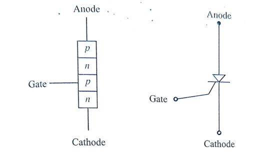
5. Thyristor
The structure of thyristor consists of four alternate p-and n-type layers. In the thyristor (also called a silicon-controlled rectifier-SCR) connections are made available to the inner layers. It acts like two transistors in tandem, one pup, and another npn. The figure shows the circuit symbol for the SCR.
The usefulness of the gate terminal rests on the fact that the current introduced into the gate may be used to control the anode-to-cathode breakover voltage. In the Fig given below the volt-ampere characteristic of an SCR is shown for various gate currents It can be observed that the firing voltage is a function of the gate current, decreasing with increasing gate current and increasing when the gate current is negative and consequently in a direction to reverse-bias the cathode junction. The current after breakdown may well be larger by a factor of 1000 than the current before breakdown. When the gate current is very large, break over may occur at so low a voltage that the characteristic has the appearance of a simple pn diode.
Suppose that a supply voltage is applied through a load resistor between the anode and cathode of an SCR. Consider that the bias is such that the applied voltage is less than the breakover voltage. Then the rectifier will remain off and may be turned on by the application to the gate of a triggering current or voltage adequate to lower the breakover voltage to less than the applied voltage. The rectifier having been turned on, latches, and it is found to be impractical to stop the conduction by reverse-biasing the gate. For example, it may well be that the reverse gate current for turn-off is nearly equal to the anode current.
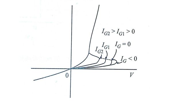
Because of its high speed, a thyristor is easily triggered by a small voltage signal (5 V, 0.1 mA). To prevent wrong operation it is customary to design the circuit so that the tripping signal will not trigger the thyristor unless it lasts for at least 2 mS. This prevents operation on interference spikes since they are momentary in nature (of the order of microseconds).
6. Logic Circuits
The concept of static relaying can be better understood by considering the logic operations performed by the devices rather than the actual happenings that occur during their operation. This makes complex static relay operations also simple, because the interest then is only on what happens rather than how it happens, and the logic part of the operation is independent of devices used to realize the events dictated by the logic.
All relays are bistable devices, le., they have two stable states, either they operate or they do not operate. Consequently, Boolean algebra can be applied to study and analyze protection schemes consisting of several relays. Using these techniques simplified block schemes can be drawn according to the logical functions performed by the various units.
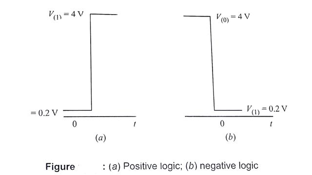
In a d.c. or level-logic, system a bit is implemented as one of two voltage levels, The more positive voltage is the 1 level and the other is the 0 level, the system is said to employ d.c. positive logic. On the other hand, a D.C. negative logic system designates the more negative voltage state of the bit as the 1 level and the more positive as the 0 level. The figure given below illustrates these two types of logic systems. Positive logic is usually followed.
(a) Basic Operations
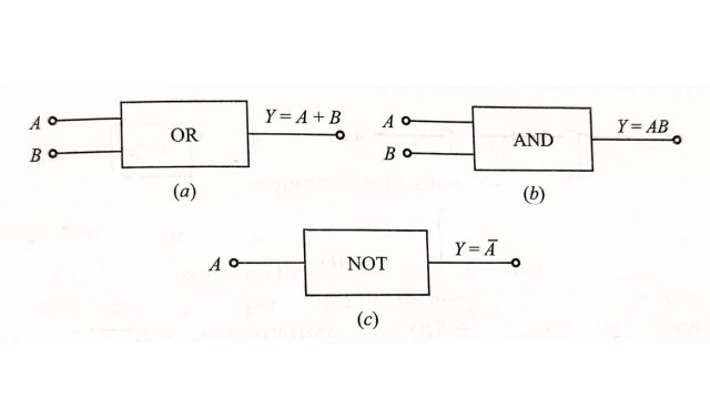
The three basic operations of Boolean algebra are:
(1) Logical sum-OR circuit.
(ii) Logical product-AND circuit.
(iii) Negation NOT circuit.
The output of an OR assumes the 1 state if one or more inputs assume the 1 state The output of an AND assumes the 1 state if and only if all the inputs assume the state.
The output of a NOT circuit takes on the 1 state if and only if the input does not take on the 1 state.
These basic operations are represented block schematically in Fig. along with their truth table which contains a tabulation of all possible input values and their corresponding outputs. Different combinations of these circuits can result in other logic circuits such as NOR and NAND circuits.
(b) Relay Logic
To start with, to make a connection between relay circuits and their logic operations, the basic operations mechanized using relays are shown in Fig. All contacts are shown in their normal position, ie., de-energized position. Thus each relay operation could be subdivided into basic switching functions which in turn can be represented by a suitable logic circuit.
In the following section, it will be shown that these logic circuits can be obtained using semiconductor devices such as diodes or transistors.
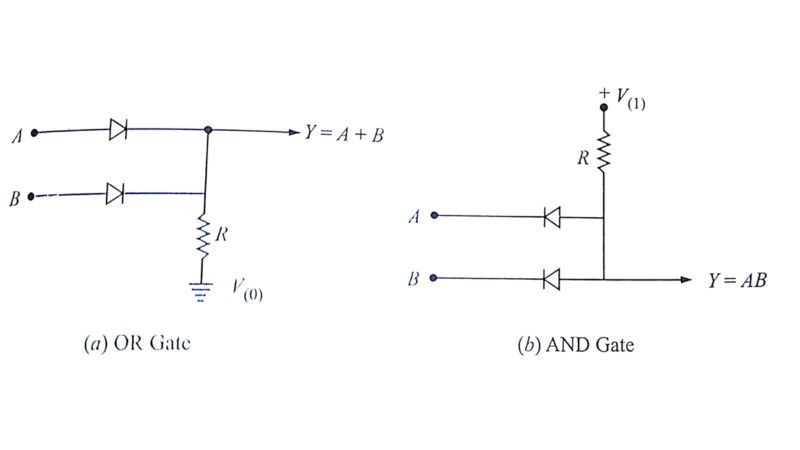
(c) Diode Logic (DL)
The two stable states of the diode are conducting (i.e., forward bias) and nonconducting (i.e., reverse bias) states. Conventional diode OR gate (circuit) and AND gate are shown in Fig.
One of the disadvantages of diode logic is that negation cannot be performed using diodes and this is where transistors are helpful.
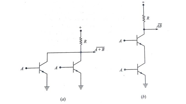
(d) Transistor Logic
Several logic circuits can be designed using transistors, especially because of the two types (npn and pnp types). Logic circuits using transistors could be developed in two forms, viz. resistor transistor logic (RTL) and direct coupled transistor logic (DCTL).
Basic NAND and NOR circuits based on the latter scheme (DCTL) are shown in Fig.
The RTL class of circuits was developed to achieve improved stability of operation. In addition, it simplifies the general gate circuitry and does not require stringent control of transistor parameters. Commonly used RTL circuits are shown in Fig. (10.23).
By using capacitances across the input resistors, the switching speed of the circuit can be increased. In such a case they are called resistance capacitance transistor logic (RCTL).
7. Smoothing Circuits
The rectified a.c. consists of a series of unidirectional half-waves of current or voltages. It is generally desirable to smooth this output. The various filters used for smoothing are the conventional RC filter, RC chain filter, transistorized filter, bucking transformer filter, phase splitting circuits, etc., some basic filter circuits are shown in the Fig given below. In the bucking transformer filter, a transformer is used to cancel out the a.c. component. This method is not suitable where the input is limited because the primary winding provides a low resistance shunt path for the d,c. diverting it from the output.
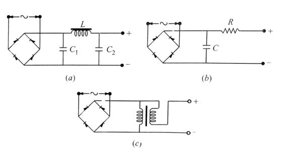
If the speed requirement is not too stringent conventional cap[acitor filters could be used. A faster method is phase splitting before rectification where the input single phase quantity is split into a multiphase system and thus greatly reduces the harmonic circuit current after smoothing.
8. Voltage Regulators
It has already been pointed out that many diodes are designed and constructed for operation on the breakdown (avalanche) portion of the characteristic curve. These diodes are known as zener diodes or reference diodes. As is obvious from their characteristics they are used for holding a voltage constant over a wide range of applied voltage. A simple circuit is shown in Fig.
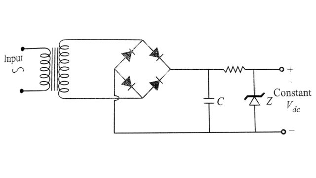
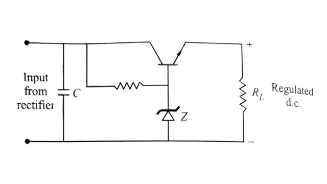
One or more transistors can be used in conjunction with the reference diode, however, to greatly increase the efficiency of the regulator by reducing the current through the reference diode. A typical circuit of this type is shown in Fig. This circuit is known as the emitter-follower regulator because the output voltage follows the reference voltage. Filters are also introduced to reduce the ripple in the output wave.
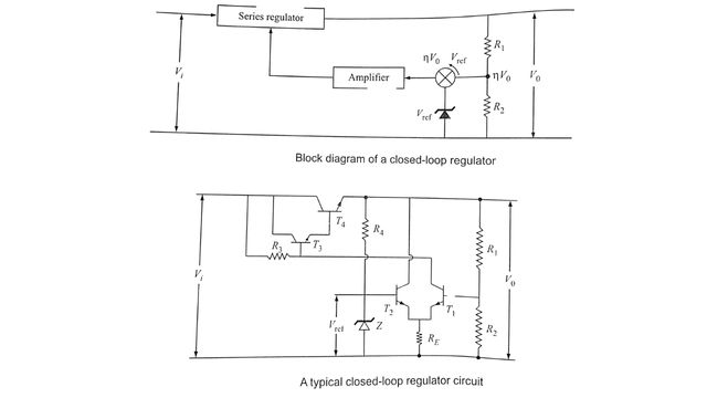
Although the emitter-follower regulators provide satisfactory performance for many applications their output resistance cannot be reduced below a particular limit, and a large value of filter capacitance (CF) is required to provide very low values of ripple. On the other hand, regulators that employ the principle of negative feedback can provide almost any desired value of output resistance and ripple quite easily. The block diagram of a closed-loop regulator is shown in Fig fraction of the output voltage V is compared with the reference voltage Vreb, and their difference is amplified and used to control the series regulator, which in turn controls the output voltage.
A typical circuit diagram that will perform this basic function is shown in Fig. The differential amplifier consisting of T1 and T2 provides both the voltage comparison and the amplification functions.
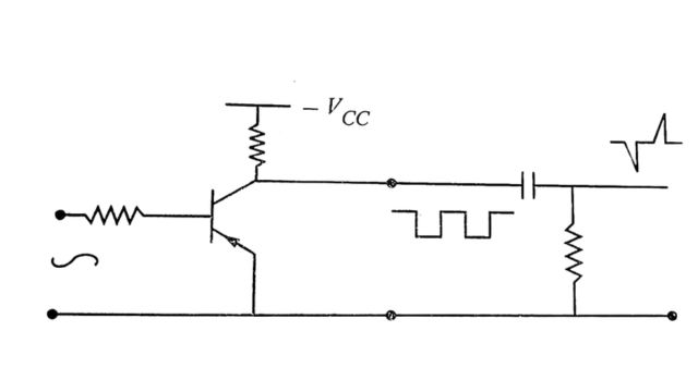
9. Square – Wave Generators
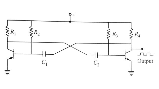
Diode clippers can be used to remove the curved portion of the sinusoidal wave to give square waves. The operational amplifier together with an integrator, can be used to generate a square wave. The simplest form of the square wave generator is the astable multivibrator shown in Fig. where two junction transistors are cross-coupled. The transistors conduct alternately with very fast regenerative transitions owing to the cross-coupling capacitors. The circuit is symmetrical if tilde R2 = R3, R1 =R4, and C1 = C2 rectangular voltage waveform can be obtained across either of the collector load resistors.
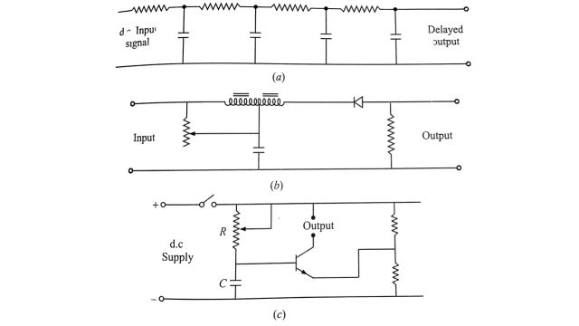
10. Time Delay Circuits
A variety of time delay circuits are available such as delay lines, resonant circuits, RC circuits, timer circuits employing transistors, thermistors, etc. The order of time delay provided by each is different, e.g., a delay line is generally used to provide very short delays of the order of microseconds; for medium delays of the order of ms, a resonant circuit is used; RC circuits are more common for longer delays. Time delays of the order of minutes or even hours are possible with RC circuits
11. Level Detectors
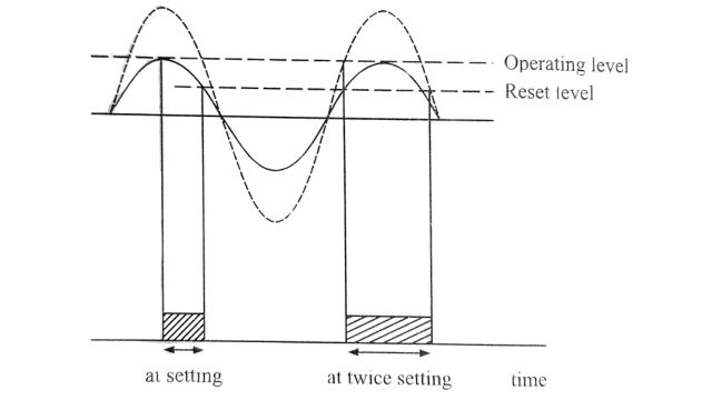
The critical level detector compares an alternating or unsmoothed rectified signal against a d.c. datum, and is intentionally designed to have a low reset ratio. For peak inputs below the datum, the output is zero, but at the critical peak input, there is a finite output pulse, the width of which is determined by the reset ratio as illustrated for the half-wave case in Fig.
The simplest form of level detector is shown in Fig. where the input voltage must exceed the opposing bias voltage before any output is produced.
A practical self-energized circuit using these principles is shown in Fig. The full wave unsmoothed input signal feeds two alternative paths I1 and I2. Below the critical level the measuring and switching circuit is fully conducting, so that the current I2 is for all practical purposes zero. The datum Vz derived from the zener diode Z1, is substantially d.c. at the critical input level. The loading on the input circuit, up to the critical level is controlled solely by Ry, which provides the voltage for the measuring and switching circuit through R1R2. The critical level occurs when the voltage across R1 exceeds Vz by the small amount of ΔV required to operate the switching circuit, which then switches to a high output impedance and diverts the current I2 into the pulse-integrating circuit. At the instant of switching the input through R1 increases to a value dependent on the input impedance of the pulse-integrating circuit, relative to R3. This provides positive feedback to the measuring circuit, which controls the instantaneous reset level. The choice of this reset level is a compromise between the extraction of reactive power from the CT and other requirements, such as transient-free properties.
12. Summation Devices
Summation transformers and sequence networks as already discussed in Chapter 2 can combine several electrical quantities into a single quantity.
The operational amplifier is commonly used as a mixer or summer as shown in Fig. The arrangement is used to obtain an output which is a linear combination of several input signals.
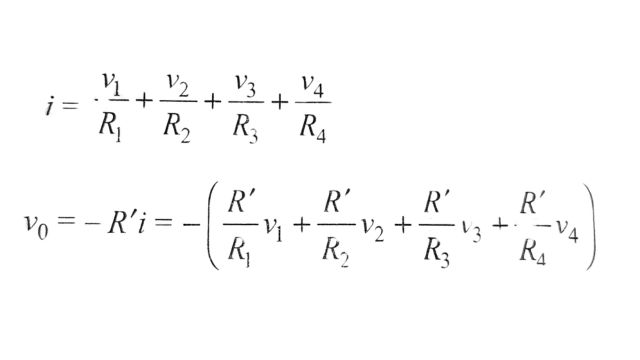
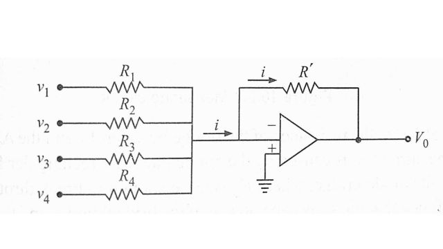
Any desired number of inputs can be used. If a simple summer or adder operation is desired, then R1 = R2 = R3 R4 = R‘, such that
v0 = ( v1 + v2 + v3 + v4)
Many other methods may, of course, be used to combine signals. The present method has the advantage that it may be extended to a very large number of inputs requiring only one additional resistor for each additional input. The result depends, in the limiting case of large amplifier gain, only on the resistors involved, and because of the virtual ground, there is a minimum of interaction between input sources.
13. Sampling Circuits
The sampling technique allows a comparison of instantaneous values derived at different instants of time, thereby dispensing with the need to phase shift and mix signals derived from the primary line quantities.
Figure shows a sampling circuit in conjunction with an amplitude pulse width converter (A/W convertor), this complete circuit forms the measuring unit for a relay. The circuit works as follows.
When iG is zero, a very high impedance is inserted between the signal voltage VS and A/W convertor. The maximum Vs must be less than the breakdown voltage of the zener diode, otherwise, conduction can take place via the Zener diode and the VG source impedance. When it is non-zero, ie., during the 50 µs sampling period source impedance. When it is non-zero, ie., during the 50 µs sampling period
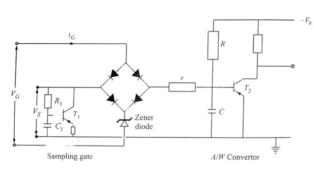
provided that iS < iG the resistance of the bridge between VS and the A/W converter is small. The current iG is caused by the application of a rectangular 50 µs voltage pulse VG to the diode bridge, where VG is large enough to break through the Zener diode. It is found that the stray capacitance of the bridge diodes and the Zener diode is such as to allow a very fast positive going edge to produce a spike at the output, even though iG is zero. The circuit comprising T1, R1, and C1 is added to deal with this contingency. The time constant R1 C1 is such that T1 is held off except when VS attempts to increase rapidly. Purely considerations cause and effect this circuit cannot remove a spike from VS, but by switching on T1 and drawing a spike of current through the signal source impedance, the rate of rise of discontinuity is slowed down sufficiently to prevent it from getting through the diode bridge.
During the 50 µs sampling period, C charges up through the resistance r + RS where RS is the signal source resistance. R >> r + RS and can therefore be neglected during the charging period. At the end of the sampling period, C commences to discharge through R towards the negative supply voltage. The diode bridge resistance is now very much larger than R and can be neglected during the discharge period. The transistor T2 is normally on and is switched off at the start of the sampling period as the voltage on C goes positive. It switches on again when the voltage on C is approximately zero. The output at the collector of T2 is therefore a pulse of length T‘ which is proportional to VS at the instant of sampling provided that T << CR.
14. Zero Crossing Detector
It involves the sine-to-square wave conversion by a level detector circuit followed by a pulse circuit, which consists of a shot monostable circuit or a differentiator. The zero crossing detection is associated with the production of a pulse at the particular zero crossing. The figure shows the circuit for the zero-crossing detector.
15. Output Devices
The output devices have to perform many duties such as operation of breaker, intertripping, alarm and remote indication, etc. Noncritical switching units are most suitable as output devices since they are associated with two or more electrically separate contact operations.
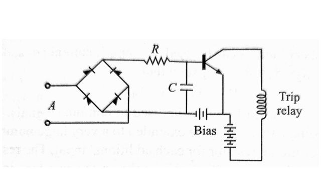
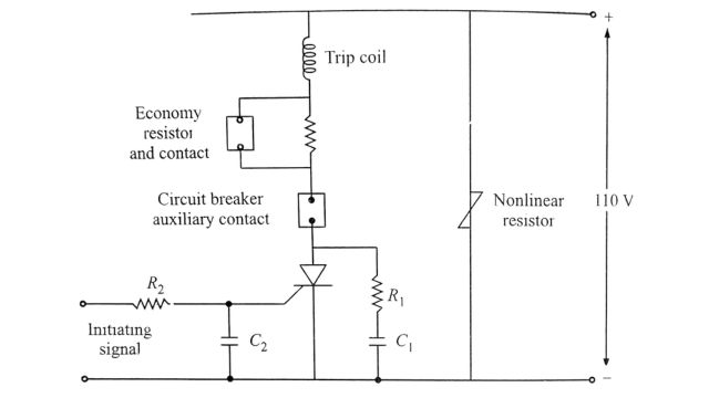
Amongst the static units, the thyristor is an excellent means for tripping the circuit breaker from a low-power signal of short duration. It operates with signals of microsecond duration but once triggered stays in conduction until broken by a switch. A typical thyristor tripping circuit is shown in Fig. R1 and C1 is included to prevent excessive surges appearing across the thyristor. The small resistance R1 limits the capacitor-discharge current or operation. The filter circuit connected to the gate electrode has the capacitor C2 connected immediately adjacent to the thyristor, to minimize pickup voltages on the gate electrode.
Reed relays though not static strictly speaking are very much suitable for semiconductor circuits. If properly designed they can also perform fast tripping of a circuit breaker, provided the power factor and ratings of the trip circuit are specified. The reed relays being very light in weight are susceptible to maloperation due to shock and vibrations.
Frequently Asked Questions (FAQs)
-
What do you mean by comparator?
A comparator circuit is like a judge deciding which of two contestants is taller. It looks at both contestants (voltages), and whichever one is taller (has a higher voltage) gets a thumbs-up (output of 1), while the shorter one (lower voltage) gets a thumbs-down (output of 0). It’s handy for figuring out if something has reached a certain level, like seeing if a cup is full or a battery is charged enough.
-
What is a sampling circuit?
A sample and hold circuit in electronics takes a snapshot of a changing voltage and keeps it steady for a while. It’s like freezing a moment in time.
-
What is a static differential relay?
A static differential relay in electrical engineering detects faults by comparing currents entering and leaving a system. It triggers if the difference exceeds a set threshold, indicating an abnormality.
Read Also:
- Electrical Cable | Components, Types and Application
- Distribution Systems | Classification and Challenges
- Transmission Line | Introduction, Classification, and Modelling
- Parallel Operation Of 1 Phase/ 3 Phase Transformers
- Power Quality | Sources Of Pollution, Need, and Effects


Leave a Reply