

Table of Contents
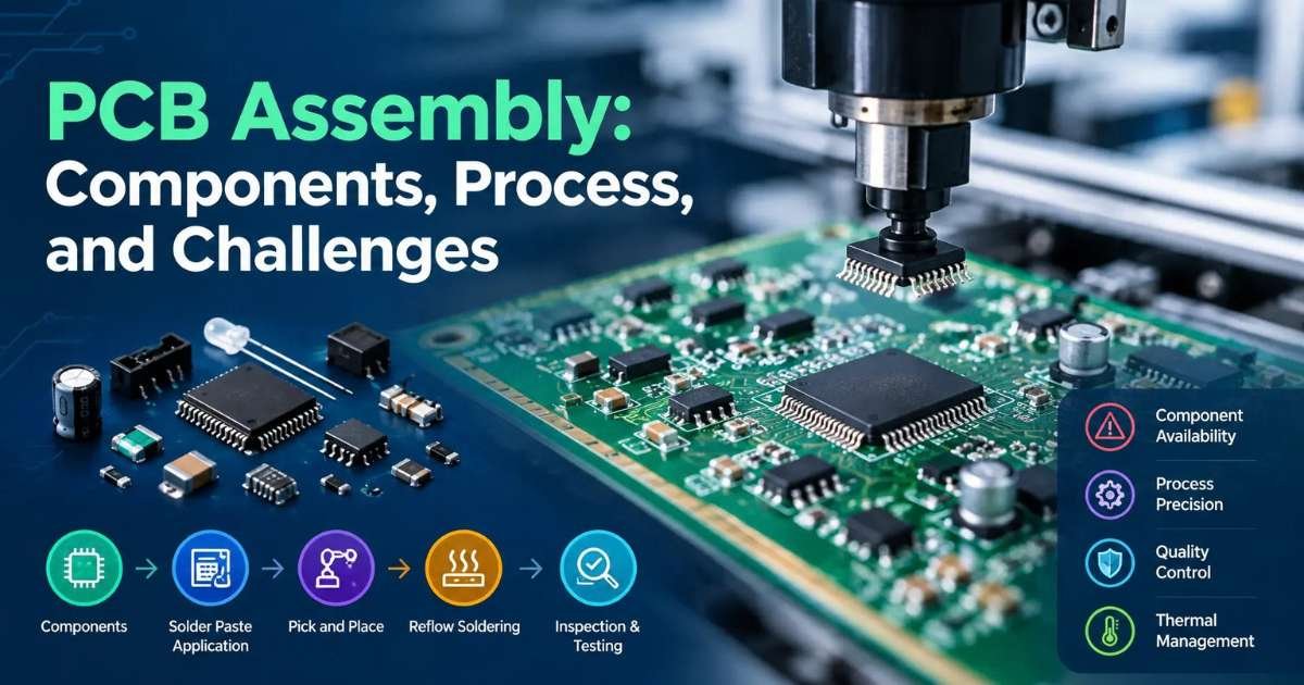
A bare printed circuit board becomes a working electronic assembly once components gets mounted on it and connected through solder joints. PCB assembly is the process of taking that empty board and turning it into a functional unit thats usable inside a electronic product.
The work involves alot more then just putting parts in there assigned positions. the manufacturer has to work with the correct components, apply solder, control the heating process and inspect the finished board for defects. Each stage can affects the performance of the final assembly.
Components Used in PCB Assembly
The PCB itself form’s the base of the assembly. The substrate carry copper traces that connect every component. Those traces determine how signals and power travels in the board. The type and arrangement of components placed on those path’s depend’s on what the finished product need’s to do.
Some of the main components and materials used during PCB assembly include :
- Bare PCB Substrate: The copper clad base layer that carry’s all electrical connections.
- Surface-Mount Components: Resistors, capacitors, diodes, transistors and integrated circuit’s can be mounted onto the board surface. There compact size make’s them suitable for packed circuit design’s.
- Through-Hole Components: These part’s have leads that pass through drilled holes in the PCB. Connectors, large capacitors, transformers and other mechanicaly stressed parts uses this mounting method.
- Solder Paste and Flux: Materials that bond components to the board and support clean electrical connection’s.
- Adhesives and Coatings: Used for component stability and protection against moisture or vibration.
We cant call these components a standard max in every board it varies from one board to another. You may see a PCB containing a few dozen components, while another one is packed with thousands of individual part’s in a small area. The manufacturer matches the PCB assembly component’s and materials with the required board design.
PCB Assembly Process
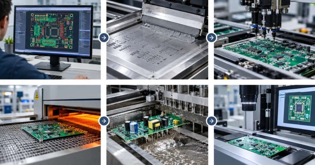
Production run’s through several distinct stages, each stage build’s on the one before it. Skipping or rushing any step usualy show’s up as a defect somewhere down the line.
Design for Manufacturing Review
The board layout get’s checked against real world manufacturing limit’s before any physical work begins. This step catches spacing issues and footprint mismatch’s. it also spot’s routing problem’s that could lead to expensive rework later on.
Solder Paste Printing
Solder paste is applyed to the PCB through a stencil for surface mount assembly. The stencil has openings that line up with the boards solder pads, so the machine can deposit paste where its needed.
Special emphasis is put on paste volume too much can cause solder bridges between neighbouring pads while too little may produce weak joint’s.
Component Placement
Pick and place machines position component’s onto the paste with impressive speed and accuracy. High volume line’s handle thousand’s of placements per hour.
Reflow Soldering
The board passes through a reflow oven, it involve’s controlled heating to melt the solder paste and form permanent electrical connections. The temperature profile has to suit the board and the component’s being used.
Through-Hole Soldering
Boards that include through hole component’s require a additional soldering step. Manufacturer’s may use wave soldering or selective soldering to connect the leads passing through the PCB.
Inspection and Testing
Automated Optical Inspection scans for misaligned or missing part’s. similarly x ray inspection checks hidden joints underneath components.
Functional testing confirm’s the board actualy performs as designed. Final cleaning remove’s leftover flux before the boards move to packaging.
Common Challenges in PCB Assembly
Component sourcing often cause’s delays in PCB assembly due to global shortages and long lead times. Part obsolescence can stall a production run for weeks. building flexibility into the bill of materials early on helps but supply chain surprises still catch seasoned teams off gaurd.
Design flaws usualy surface when manufacturing begins. We’ve seen that a trace routed too close to a pad or a footprint that doesnt quite match the component datasheet send’s a entire batch back for rework. Teams that catch these problem’s during the design phase can save time and money.
Soldering defects remain a persistant headache. Bridging occurs when solder connects two pads that should stay seperate, while tombstoning happens when a component lift’s at one end during reflow. Cold solder joints caused by insufficient heat can create connections that look fine visualy, however they fail electricaly over time, sometimes months after the product ships.
Coordinating separate vendors adds another layer of risk. One company may fabricate the PCB, another may provide the components and a third may assemble the finished boards. So imagine a miscommunication between a fab house and a assembler, which could mean a board arrives with the wrong hole size’s or copper thickness. Plus nobody notice’s until PCB assembly is already underway.
How Turnkey PCB Assembly Can Simplify Production
Turnkey PCB assembly puts sourcing, fabrication, assembly and testing under a single providers roof. this gives the project team one place to handle production question’s.
Communication improves because one team own’s the entire pipeline. Component substitution’s and quality concerns get resolved fast, without the back and forth of routing questions between separate companies.
Quality control becomes consistant too. A turnkey PCB assembly provider inspect’s boards at every stage under one unified standard. This is crucial for startups and lean engineering teams that lack dedicated procurement staff to chase down suppliers or verify component authenticity.
Turnaround time’s shrink as well, since the provider manages inventory and scheduling internaly without waiting on shipment’s from separate fab houses and component distributors.
Simply put a single manufacturing partner can help carry the project through various production stages while maintaining consistant specifications and quality requirements.
Final Thoughts
PCB assembly turns a bare board into a functioning part of an electronic product. its a layered process that involve’s careful component selection with precise machine work and thorough inspection at every stage.
Production challenges can appear at any stage it can be related to sourcing a hard to find component or catching a soldering defect. However teams that choose a turnkey PCB assembly partner with suitable equipment and production experience see’s fewer delays/defects and a smoother path from prototype to large scale manufacturing.





Leave a Reply