Table of Contents
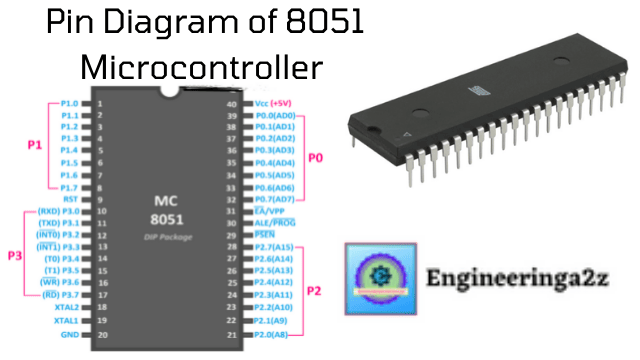
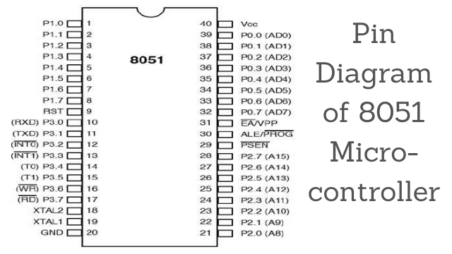
Pin Diagram of 8051
The 8051 microcontroller has 40 pins of dual-in-line packaging and is an 8-bit microprocessor. I/O ports occupy 32 out of the 40 pins available. In the 8051, however, there are multiple pins with multiple signals allocated to them.
The pin diagram for the 8051 microcontroller is shown below:
Explanation of each pin of 8051 Microcontroller is as :-
Vcc
It is Pin 40 used as power supply pin to which the supply voltage is given (+5V).
Vss
The 8051 microcontroller’s ground pin is pin 20. It is attached to the power supply’s negative terminal (0V) and represents 0V.
Port 0
PORT 0 pins are pins 32 to 39. They’re bidirectional input/output pins. It is 8 bit open drain bidirectional input output port.
It is configured as multiplex low order address and data bus.
Port 1
Pins 1 to 8 are the 8051’s PORT 1 pins. PORT 1 pins is a bidirectional 8-bit input/output port with inbuilt pull-up resistors. It is 8 bit bidirectional input output port with internal pull up register.
Port 2
From pin 21 to 28 these are the PORT 2 pins of the 8051 microcontroller. It is 8 bit bidirectional input output port with internal pull up register.
It carries higher order address (A8-A15)
Port 3
It is 8 bit bidirectional input output port with internal pull up register.
It can perform various other functions as :-
RXD
It is on pin 10. This is serial receive port. which is used for serial input. The microcontroller gets data for serial communication via this input signal.
TXD
It is on pin 11. This is serial transmit port. which is serial output pin. Through this output signal microcontroller transmits data for serial communication
INT0
It is on pin 12. It is external interrupt 0
INT1
It is on pin 13. It is external interrupt 1
Timer T0
The timer T0 is virtually 16-bit register. Two registers TMOD and TCON are closely connected to this timer and control its operation. Timer 0 is on pin 14
Timer T1
In the timer mode, the internal machine cycles are counted. So this register is incremented in each machine cycle. Timer 1 is on pin 15
WR
It is external write device pin. It is on pin 16
RD
It is external device read pin. it is on pin 17
Reset
Pin 9 is the Reset Input Pin. when reset pin is high then all the register reset to their initial value.
PSEN
It is on the 29 pin. Which stand for Programme Store Enable. When it low then microcontroller reads data from external programme memory.
EA/VPP
Pin 31 is EA pin which stands for External Access Pin. It is active low pin. When it is zero then external ROM is used to read code byte. When this pin high then internal Rom is used to read code byte.
ALE/PROG
Pin 30 is Address Latch Enable. When this pin is high then it works as address latch enable mode & when this pin is low it works as a programming code memory (ROM).
Crystal XTAL1 – XTAL2
This are connected on Pins 18 and 19. This are the pins for connecting external oscillator. Generally a Quartz Crystal Oscillator is connected here.
Frequently Asked Questions (FAQs)
-
What is ALE?
It stand for Address Latch Enable. When this pin is high then it works as address latch enable mode & when this pin is low it works as a programming code memory (ROM).
-
What is the function of VCC?
In 8051, EA is connected to Vcc as it comes with on-chip ROM to store programs. It is used to enable/disable external memory interfacing.
-
What is the function of Timers in 8051?
The 8051 has two counters/timers which can be used either as timer to generate a time delay or as counter to count events happening outside the microcontroller.


Leave a Reply